Silicon Photonics and Optical Interconnects: Overcoming the AI Datacenter Bandwidth & Power Wall in 2026
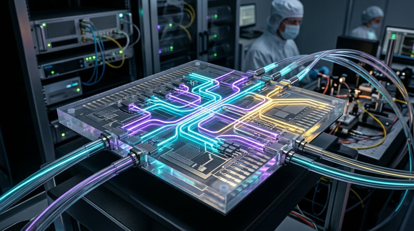
Quick Answer: The exponential scaling of frontier artificial intelligence models has collided with a fundamental physical barrier: the Copper Interconnect Wall. In multi-thousand GPU superclusters, electrical copper wiring generates catastrophic thermal dissipation and signal attenuation over distances as short as two meters, consuming up to 30% of total datacenter energy solely for data transport. In 2026–2027, the commercial maturation of Silicon Photonics and Co-Packaged Optics (CPO) replaces electrical copper electrons with coherent laser photons routed directly onto semiconductor packages. This transition delivers a 10x reduction in transmission energy (sub-picojoule per bit), eliminates network latency bottlenecks, and enables exascale distributed AI training architectures.
As artificial intelligence models scale past tens of trillions of parameters, the limiting constraint of datacenter engineering has shifted from raw compute (FLOPS) to interconnect bandwidth. Modern frontier LLM architectures and Mixture-of-Experts (MoE) networks require all-to-all communication across hundreds of thousands of accelerators at microsecond latency.
For decades, datacenter architects relied on traditional pluggable optical transceivers connected to networking switches via copper cables. However, at speeds exceeding 1.6 Terabits per second (Tbps) per lane, electrical resistance turns copper wires into miniature heaters, causing unacceptable signal degradation and thermal throttling.
Silicon photonics fundamentally solves this bottleneck by fabricating microscopic optical waveguides, modulators, and photodetectors directly on standard silicon CMOS foundry wafers, transmitting data at the speed of light.
Architectural Evolution: Electrical Copper vs. Co-Packaged Silicon Photonics
To understand how silicon photonics redefines supercomputer networking, examine the architectural transformation occurring across GPU racks:
Legacy Electrical Copper Interconnect (Thermal & Distance Limited):
[GPU Die] ──► [Long Electrical PCB Trace] ──► [Pluggable Transceiver] ──► [Copper Cable]
                  │ (High Heat Dissipation & 15-25 pJ/bit Energy Loss)
                  ▼
          (Signal Attenuation at >1.6 Tbps Across >2 Meters)

Co-Packaged Optics (CPO) Silicon Photonics Architecture:
[GPU Compute Chiplet]
         │ (Ultra-short sub-millimeter die-to-die bridge)
         ▼
[Silicon Optical Engine (Waveguides + Micro-Ring Modulators)]
         │ (Coherent multi-wavelength laser light)
         ▼
[Direct Optical Fiber Interconnect (Sub-1 pJ/bit across 100+ meters)]
Strategic Comparison Matrix: Electrical Copper vs. Silicon Photonics Interconnects
The table below contrasts the operational and physical characteristics of copper cabling against next-generation silicon photonic interconnects:
| Metric / Architectural Feature | Legacy Direct Attach Copper (DAC) | Co-Packaged Optics (CPO) Silicon Photonics |
|---|---|---|
| Energy Consumption per Bit | 15 to 25 picojoules per bit (pJ/bit) | 1.0 to 2.5 picojoules per bit (sub-pJ in next-gen) |
| Maximum High-Speed Reach | < 2 meters at 800G / 1.6T (severe degradation) | > 100 to 500 meters without active repeaters |
| Cable Bulk & Weight | Extremely heavy, rigid copper harnesses blocking rack airflow | Lightweight, flexible, microscopic fiber-optic ribbons |
| Latency Characteristics | Higher serialization latency due to complex DSP Retimers | Speed-of-light optical flight time; eliminates DSP retiming |
| Manufacturing Foundry Process | Separate specialized copper extrusion and assembly | Standard CMOS silicon semiconductor foundries (TSMC / Intel) |
| Datacenter Cooling Impact | Requires intense fan power and liquid-assisted cooling | Dramatically lower thermal load, direct cold-plate liquid cooling |
Core Breakthroughs Driving Silicon Photonics in 2026–2027
Three fundamental technological breakthroughs have transitioned silicon photonics from experimental physics labs into mainstream production datacenters:
1. Co-Packaged Optics (CPO) and 2.5D/3D Packaging
Historically, optical transceivers were bulky modules plugged into the front faceplate of network switches. The electrical signal had to travel across centimeters of lossy PCB traces before conversion into light. CPO eliminates this trace distance by mounting the silicon optical engine directly onto the same substrate interposer as the GPU or switch ASIC. By shortening the electrical path to less than 1 millimeter, CPO reduces I/O power dissipation by more than 70%. (Read our analysis on Neuromorphic Chips and Edge Computing.)
2. Multi-Wavelength Micro-Ring Resonators
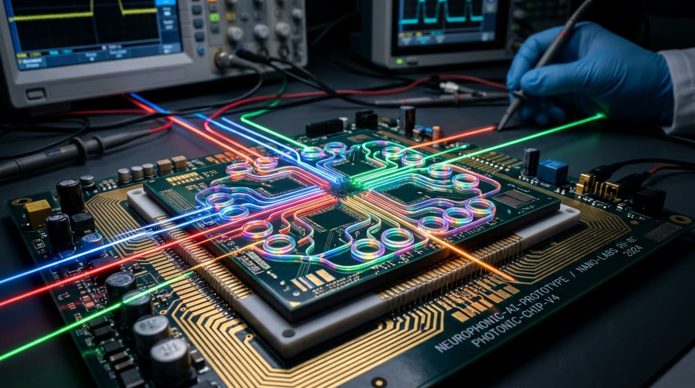
To maximize bandwidth without multiplying physical fiber count, modern photonic engines utilize micro-ring resonators for Dense Wavelength Division Multiplexing (DWDM). A single optical waveguide simultaneously transports 16 to 32 discrete laser wavelengths of light, each operating at 100 Gbps, enabling a single fiber strand to carry 3.2 Terabits per second of bidirectional bandwidth with zero cross-talk interference. (Explore our research on Optical Neural Networks and Photonic AI.)
3. Continuous External Laser Sources (ELS)
Early optical chip architectures suffered from laser reliability issues caused by the extreme heat generated by neighboring compute dies. The 2026 industry standard decouples laser generation by using blind-mate External Laser Source (ELS) pluggable modules mounted on the cooler front chassis, piping clean continuous-wave (CW) laser power into the compute package via polarization-maintaining fibers. If a laser diode fails, it can be hot-swapped in seconds without interrupting GPU execution.
Datacenter Macro Impact: Power PUE and Megawatt Conservation
For hyperscalers and sovereign AI infrastructure operators, silicon photonics is an operational survival imperative:
- Escaping the Datacenter Power Grid Cap: Modern gigawatt-scale AI campuses are constrained by local electric utility grid allocations. By trimming 15 to 20 picojoules per bit across tens of petabytes of continuous East-West cluster traffic, silicon photonics conserves tens of megawatts of electrical power—redirecting that energy directly into training compute capacity. (Explore our macro analysis on Sovereign AI Infrastructure as an Asset Class.)
- True Memory Disaggregation (Optical CXL): With sub-nanosecond optical flight times, GPUs can access disaggregated pools of High Bandwidth Memory (HBM) and DDR5 across distant racks as if they resided on local memory buses, dramatically optimizing hardware utilization for giant MoE models.
- Linear Datacenter Scalability: High-speed optical links eliminate the physical radius constraints of datacenter clusters. GPU servers can be distributed across multi-story buildings and modular pods while maintaining uniform, ultra-low latency fabric connectivity.
Frequently Asked Questions (FAQ)
What is the primary difference between silicon photonics and traditional optical transceivers?
Traditional optical transceivers are discrete, pluggable modules assembled using manual micro-optics and mounted on network switch faceplates, requiring high-power electrical traces across PCBs. Silicon photonics integrates all optical components (waveguides, modulators, detectors) directly into silicon semiconductor chips manufactured on standard commercial semiconductor foundry lines, enabling massive scale, lower costs, and seamless integration alongside compute processors.
Why can't electrical copper cables simply be made thicker to handle higher speeds?
Making copper conductors thicker increases physical weight and stiffness, rendering server racks impossible to cable, while severely obstructing airflow required for cooling. More critically, at high frequencies (>100 GHz), the skin effect forces electrons to travel only on the outer surface of conductors, causing exponential attenuation that cannot be overcome by simply adding more metal.
Is silicon photonics already deployed in production commercial datacenters?
Yes. As of 2026, leading AI hyperscalers, GPU manufacturers, and networking giants (such as NVIDIA, Broadcom, Intel, and TSMC) have transitioned from lab pilots to commercial production of Co-Packaged Optics and optical transceivers operating at 1.6T and 3.2T data rates within frontier AI training clusters.
How does silicon photonics contribute to AI sustainability and carbon reduction?
Data transport and cooling represent nearly 40% of an AI cluster's parasitic electrical overhead. By cutting interconnect transmission power by up to 80% and drastically reducing thermal dissipation, silicon photonics reduces datacenter Power Usage Effectiveness (PUE) and saves millions of kilowatt-hours of annual grid electricity per supercomputer cluster.