Photonic Neuromorphic Computing: Breaking the Energy Wall in Next-Gen AI Silicon
As foundation models scale past multi-trillion parameters, semiconductor engineering faces an insurmountable physical boundary: the electronic interconnect bottleneck. While transitor density has continued to advance through sub-2nm gate-all-around (GAA) architectures, the electrical resistance and capacitance of copper wires generate crippling thermal dissipation and parasitic capacitance. In modern AI superclusters, over 60% of total system power is wasted not on tensor calculation, but merely shuttling bits across circuit boards.
Photonic neuromorphic computing represents the quantum leap required to break this energy wall. By replacing copper wires and electrical electrons with directed photons travelling across silicon waveguides at the speed of light, optical computing processors perform linear matrix mathematics with near-zero heat and sub-picosecond latency.
How Optical Neuromorphic Chips Compute with Light
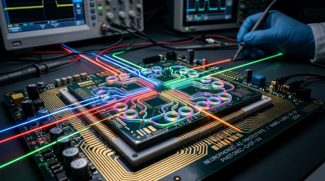
At the core of an optical neural processor lies the silicon photonic integrated circuit (PIC). Rather than performing floating-point operations through billions of silicon logic gates switching on and off, photonic processors manipulate the fundamental wave properties of light—such as phase, amplitude, and wavelength.
1. Mach-Zehnder Interferometer (MZI) Meshes
Optical matrix multiplication is physically executed through programmable grids of Mach-Zehnder Interferometers. By applying microscopic thermal or electro-optic phase shifts, incoming coherent laser beams interfere constructively or destructively. This physical optical interference executes arbitrary unitary matrix transformations instantly as light passes through the glass waveguides.
2. Micro-Ring Resonators (MRRs) and WDM
Wavelength Division Multiplexing (WDM) enables hundreds of discrete optical carrier signals—each on a subtly different color wavelength—to travel simultaneously down a single microscopic silicon waveguide. Micro-ring resonators filter and modulate these wavelengths with sub-micron precision, allowing parallel matrix convolutions without physical wire congestion.
3. Co-Packaged Optics (CPO)
Traditional AI accelerators lose enormous energy driving electrical signals through PCIe lanes and copper SerDes cables. Co-packaged optics mounts photonic transceivers directly onto the same substrate as advanced compute silicon, eliminating heavy copper traces and reducing interconnect power dissipation by upwards of 75%.
Performance Comparison: Silicon Photons vs. Classical Electrons
| Benchmark Metric | Classical High-End GPU / TPU | Photonic Neuromorphic Accelerator |
|---|---|---|
| Compute Latency (MAC unit) | 0.5 – 1.5 nanoseconds | < 1.0 picosecond (flight of light) |
| Energy Consumption | ~10–50 Picojoules / FLOP | ~0.05–0.2 Picojoules / MAC |
| Interconnect Bandwidth | Copper SerDes limited (~1.6 Tbps) | Optical Waveguide (> 100 Tbps aggregate) |
| Heat Dissipation at Peak Load | Extreme (Requires Liquid Nitrogen / Direct Chilled Water) | Low (Thermal dissipation isolated to laser sources) |
| Signal Attenuation | High RC delay over centimeters | Negligible attenuation across datacenter racks |
Strategic Real-World Applications
1. Real-Time Autonomous Defense & Radar Signal Processing
Phased-array radar systems and electronic warfare suites generate millions of raw radio-frequency (RF) samples per millisecond. Electronic microprocessors cannot digitize and process this deluge without severe latency. Photonic processors convert analog RF waves directly into optical signals, identifying hostile radar chirps and navigational threats instantly.
2. Hyperscale Transformer Inference at Macroeconomic Scale
Running frontier multi-modal reasoning models creates massive municipal grid strains. Hyperscale datacenters adopting photonic accelerators can operate continuous real-time video and audio inference engines within standard electrical substation envelopes, cutting operational cooling budgets by millions of dollars annually.
3. Neuromorphic Ultra-Low Power Edge Sensors
Miniaturized optical chips integrated into medical endoscopy sensors, satellite telemetry pods, and smart robotic joints can classify sensory input locally without transmitting unencrypted raw data packets over vulnerable radio connections.
Frequently Asked Questions
Can photonic processors perform general-purpose computing like a standard CPU?
No. Photonic hardware is an application-specific accelerator fundamentally tailored for linear algebra, Fourier transforms, and matrix multiplication. Non-linear activation functions and storage operations are still managed in hybrid co-packaged electronic layers.
What is the biggest hurdle to mass adoption of photonic chips?
Precision laser source integration, fiber-to-chip packaging alignment tolerances at the nanometer scale, and thermal drift stabilization of micro-ring resonators represent the primary industrial fabrication challenges currently being solved.
Will optical computers make GPUs obsolete?
Rather than replacing GPUs, optical processors will act as co-processors. Future compute nodes will feature hybrid architectures: high-throughput photonic engines executing heavy tensor convolutions, coupled with electronic logic handling memory coordination and system orchestration.